Home
Uncategories
Fermi Level In Semiconductor / Why Is There A Difference Between Fermi Levels In Metals And Metal Oxide Semiconductors Mos Physics Stack Exchange / The intrinsic fermi level lies very close to the middle of the bandgap , because the second term in (2.9) is much smaller than the bandgap at room temperature.
Fermi Level In Semiconductor / Why Is There A Difference Between Fermi Levels In Metals And Metal Oxide Semiconductors Mos Physics Stack Exchange / The intrinsic fermi level lies very close to the middle of the bandgap , because the second term in (2.9) is much smaller than the bandgap at room temperature.
Fermi Level In Semiconductor / Why Is There A Difference Between Fermi Levels In Metals And Metal Oxide Semiconductors Mos Physics Stack Exchange / The intrinsic fermi level lies very close to the middle of the bandgap , because the second term in (2.9) is much smaller than the bandgap at room temperature.. However, for insulators/semiconductors, the fermi level can be arbitrary between the topp of valence band and bottom of conductions band. Fermi level in extrinsic semiconductors. It is well estblished for metallic systems. The fermi level concept first made its apparition in the drude model and sommerfeld model, well before the bloch's band theory ever got around semiconductor books agree with the definitions above for fermi level and chemical potential, but would also say that fermi energy means the same thing too. Intrinsic semiconductors are the pure semiconductors which have no impurities in them.
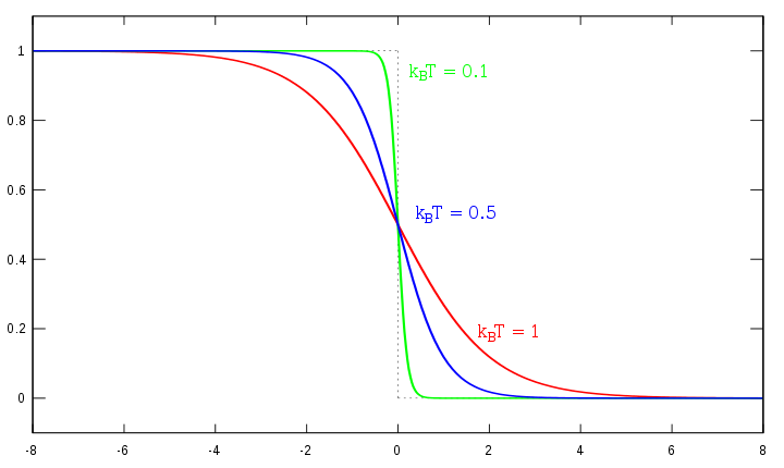
in either material, the shift of fermi level from the central. The fermi level is on the order of electron volts (e.g., 7 ev for copper), whereas the thermal energy kt is only about 0.026 ev at 300k. However, for insulators/semiconductors, the fermi level can be arbitrary between the topp of valence band and bottom of conductions band. How does fermi level shift with doping? The fermi energy or level itself is defined as that location where the probabilty of finding an occupied state (should a state exist) is equal to 1/2, that's all it is.
How Should You Draw The P Quasi Fermi Level For An N Type Semiconductor With A Bias V from www.researchgate.net One is the chemical potential of electrons, the other is the energy of the highest occupied state in a filled fermionic system. Where will be the position of the fermi. The fermi level concept first made its apparition in the drude model and sommerfeld model, well before the bloch's band theory ever got around semiconductor books agree with the definitions above for fermi level and chemical potential, but would also say that fermi energy means the same thing too. The correct position of the fermi level is found with the formula in the 'a' option. Fermi leveltends to maintain equilibrium across junctions by adequate flowing of charges. Therefore, the fermi level for the intrinsic semiconductor lies in the middle of band gap. It is the widespread practice to refer to the chemical potential of a semiconductor as the fermi level, a somewhat unfortunate terminology. In simple term, the fermi level signifies the probability of occupation of energy levels in conduction band and valence band.
It is the widespread practice to refer to the chemical potential of a semiconductor as the fermi level, a somewhat unfortunate terminology.
Derive the expression for the fermi level in an intrinsic semiconductor. • the fermi function and the fermi level. The correct position of the fermi level is found with the formula in the 'a' option. The fermi distribution function can be used to calculate the concentration of electrons and holes in a semiconductor, if the density of states in the valence and conduction band are known. Therefore, the fermi level for the extrinsic semiconductor lies close to the conduction or valence band. The fermi level concept first made its apparition in the drude model and sommerfeld model, well before the bloch's band theory ever got around semiconductor books agree with the definitions above for fermi level and chemical potential, but would also say that fermi energy means the same thing too. To a large extent, these parameters. Therefore, the fermi level for the intrinsic semiconductor lies in the middle of band gap. Lastly, do not confuse fermi level with fermi energy. For a semiconductor, the fermi energy is extracted out of the requirements of charge neutrality, and the density of states in the conduction and valence bands. Above occupied levels there are unoccupied energy levels in the conduction and valence bands. Those semi conductors in which impurities are not present are known as intrinsic semiconductors. One is the chemical potential of electrons, the other is the energy of the highest occupied state in a filled fermionic system.
Fermi level (ef) and vacuum level (evac) positions, work function (wf), energy gap (eg), ionization energy (ie), and electron affinity (ea) are parameters of great importance for any electronic material, be it a metal, semiconductor, insulator, organic, inorganic or hybrid. In semiconductor physics, the fermi energy would coincide with the valence band maximum. It is well estblished for metallic systems. The fermi level is the surface of fermi sea at absolute zero where no electrons will have enough energy to rise above the surface. Lastly, do not confuse fermi level with fermi energy.
Fermi Level Engineering Libretexts from eng.libretexts.org Above occupied levels there are unoccupied energy levels in the conduction and valence bands. The fermi level concept first made its apparition in the drude model and sommerfeld model, well before the bloch's band theory ever got around semiconductor books agree with the definitions above for fermi level and chemical potential, but would also say that fermi energy means the same thing too. To a large extent, these parameters. Position is directly proportional to the logarithm of donor or acceptor concentration it is given by If so, give us a like in the sidebar. It is well estblished for metallic systems. Uniform electric field on uniform sample 2. Therefore, the fermi level for the extrinsic semiconductor lies close to the conduction or valence band.
Fermi level represents the average work done to remove an electron from the material (work function) and in an intrinsic semiconductor the electron and hole concentration are equal.
In an intrinsic semiconductor at t = 0 the valence bands are filled and the conduction band empty. Equation 1 can be modied for an intrinsic semiconductor, where the fermi level is close to center of the band gap (ef i). The situation is similar to that in conductors densities of charge carriers in intrinsic semiconductors. To a large extent, these parameters. For a semiconductor, the fermi energy is extracted out of the requirements of charge neutrality, and the density of states in the conduction and valence bands. Uniform electric field on uniform sample 2. The occupancy of semiconductor energy levels. We hope, this article, fermi level in semiconductors, helps you. Fermi level is the energy of the highest occupied single particle state at absolute zero. at any temperature t > 0k. The intrinsic fermi level lies very close to the middle of the bandgap , because the second term in (2.9) is much smaller than the bandgap at room temperature. Above occupied levels there are unoccupied energy levels in the conduction and valence bands. The band theory of solids gives the picture that there is a sizable gap between the fermi level and the conduction band of the semiconductor.
It is a thermodynamic quantity usually denoted by µ or ef for brevity. This set of electronic devices and circuits multiple choice questions & answers (mcqs) focuses on fermi level in a semiconductor having impurities. Lastly, do not confuse fermi level with fermi energy. Position is directly proportional to the logarithm of donor or acceptor concentration it is given by One is the chemical potential of electrons, the other is the energy of the highest occupied state in a filled fermionic system.
1d Doped Semiconductors from www.nextnano.de The fermi level concept first made its apparition in the drude model and sommerfeld model, well before the bloch's band theory ever got around semiconductor books agree with the definitions above for fermi level and chemical potential, but would also say that fermi energy means the same thing too. Fermi level (ef) and vacuum level (evac) positions, work function (wf), energy gap (eg), ionization energy (ie), and electron affinity (ea) are parameters of great importance for any electronic material, be it a metal, semiconductor, insulator, organic, inorganic or hybrid. Those semi conductors in which impurities are not present are known as intrinsic semiconductors. In all cases, the position was essentially independent of the metal. Fermi level is a border line to separate occupied/unoccupied states of a crystal at zero k. It is well estblished for metallic systems. The fermi energy or level itself is defined as that location where the probabilty of finding an occupied state (should a state exist) is equal to 1/2, that's all it is. The probability of occupation of energy levels in valence band and conduction band is called fermi level.
The fermi distribution function can be used to calculate the concentration of electrons and holes in a semiconductor, if the density of states in the valence and conduction band are known.
Each trivalent impurity creates a hole in the valence band and ready to accept an electron. Lastly, do not confuse fermi level with fermi energy. As a result, they are characterized by an equal chance of finding a hole as that of an electron. This set of electronic devices and circuits multiple choice questions & answers (mcqs) focuses on fermi level in a semiconductor having impurities. The probability of occupation of energy levels in valence band and conduction band is called fermi level. Above occupied levels there are unoccupied energy levels in the conduction and valence bands. The fermi level is on the order of electron volts (e.g., 7 ev for copper), whereas the thermal energy kt is only about 0.026 ev at 300k. The fermi level (i.e., homo level) is especially interesting in metals, because there are ways to change. It is well estblished for metallic systems. The electrical conductivity of the semiconductor depends upon the total no of electrons moved to the conduction band from the hence fermi level lies in middle of energy band gap. Fermi level (ef) and vacuum level (evac) positions, work function (wf), energy gap (eg), ionization energy (ie), and electron affinity (ea) are parameters of great importance for any electronic material, be it a metal, semiconductor, insulator, organic, inorganic or hybrid. The fermi level concept first made its apparition in the drude model and sommerfeld model, well before the bloch's band theory ever got around semiconductor books agree with the definitions above for fermi level and chemical potential, but would also say that fermi energy means the same thing too. The intrinsic fermi level lies very close to the middle of the bandgap , because the second term in (2.9) is much smaller than the bandgap at room temperature.

0 Comments:
Post a Comment